Vacuum Deposition
Contact: Ken Tokunaga, 510 486-5045
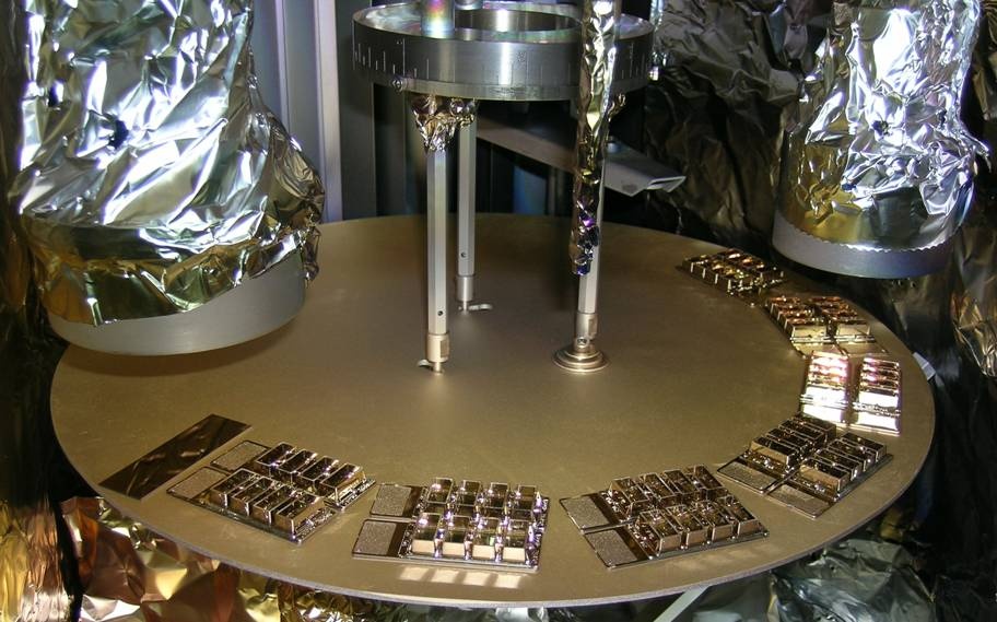
The vacuum deposition laboratory deposits many materials onto a wide array of substrates. The deposition processes include magnetron sputtering, electron beam evaporation, and resistive evaporation. These deposition processes produce ultra high purity contamination free films. The deposition processes are precisely controlled to obtain films with thickness of a few nanometers or higher on a substrate. When required film thickness and stress are measured using a metrology tool. We can also create a pattern film on substrate via masking or photolithographic techniques. The process staff will assist you in the selection of the best material, film thickness, film characteristic(s), and process for your application.
Many solid, non-radioactive elements and isotopes have been deposited. Au, Al, B, Cu, Pb, Pt, Ru, Sm, Ti, and W are a few recent examples. In addition to elements, compounds are deposited too. !CsI, !LiI, !SiO, and !TiN are examples of compound depositions. These are some film / substrate applications- pattern photoresist on nitride windows, !TiN on aluminum, Pt on kapton, Au on kapton, Ti on glass, Au on glass, !CsI on nitride window, Cu on molybdenum, Rh on beryllium, Ru on carbon foil, Au on formvar foil, and Au on plastic.